General features
Based on the interferometry technique, LEM camera is ideally suited to etch/deposition rate monitoring, Fringes counting and endpoint detection, providing high precision detection of film thickness and trench depth and also interfaces.
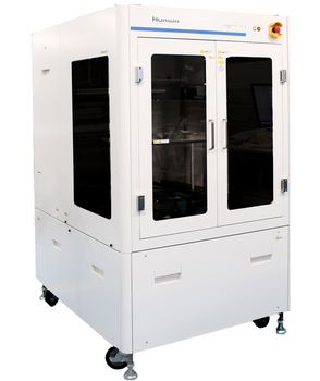
The LEM camera can be mounted on any process chamber with direct top view of the wafer and provides a real-time digital CCD image of the sample surface making spot positioning simple.

Figure 1: Camera image makes spot positioning simple
General features
- Multi-Configurations to fit your needs
LEM Camera is available with: - 2 configurations :
- LEM Sensor
- simple analog output,
- ideal for OEMs (sensor only)
- LEM-CT complete instrument
- includes full computer control (Sigma_P software) powered by an easy to use recipe editor for advanced process monitoring. Ideal for OEMs and process development in industrial R&D environments.
- 3 types of lasers compatible with a broad range of films including SiN, SiO2, GaAs, InP, AlGaAs, GaN… LEM camera uses visible (670 nm) or NIR laser (905, 980 nm) depending on applications
- XY manual or motorized stage
- Perpendicularity Tilt management on the LEM sock (default) or using an easier tilt function (optional)
- Sensor head: Camera with CCD imaging
A large objective lens to wafer distance attachment range of 200 mm to 800 mm. The use of lasers enables a spot diameter as small as 20 µm to 100 µm. A compact, self-contained amplifier design that allows simple monitoring of 0 V to 10 V outputs with only a camera if connected to devices such as a data logger.
This system calculates the etching/deposition speed of the monitored area by monitoring the interference intensity based on the cycle, leading to detection of the end-point from the prescribed film thickness and trench depth.
Based on this theory, this system is extremely stable and can be used with complex multi-layer films.
- Frame grabber
The frame grabber permits to optimize camera setup position and also to set the spot on the right location for process monitoring.
- Traditional interference wave type
The horizontal axe represents time. An interference cycle is generated with respect to the etching depth as the etching process progresses. The amount of etching during one cycle is displayed as Thickness/Depth = λ (laser wavelength) / 2n (refractive index of etching film).

- Sigma_P for real-Time Monitoring and Endpoint
�������������© software allows rapidly configuring recipe and then creating robust endpoint detection: - Using Windows 10 based Software platform, intuitive user interaction permits to deal with Laser wavelength along time.
- A simple Recipe Editor allows the user to build efficient recipes, signal arithmetic and filtering, plus Endpoint condition(s) and decision(s), using a Formula Editor, with help online integrated.
- Up to 8 curves can be displayed on the same screen to monitor Signal, derivative plus specific Interferometric Method variables & Endpoint at the same time.
- Recipe Management
Unified concept permits to setup recipes in a fluent and user-friendly Excel-like Recipe Editor.
With Sigma_P software expansion settings feature, many compatible algorithms for special signal detection and detection of signals with poor S/N ratios are included and can always be expanded.
- SQL Management
Chamber Database, Tool Databases are embedded close to the sensor and accessible online, by operator, by recipes, by statisticians, by APC servers, by distant process engineer office.
- Reprocessing Manager to playback raw data
To allow instant replay of mathematical treatment for instrumentation optimization but also scripted automatic reprocessing of multiple data runs for process validation, APC extensions, parametric studies.
This data can also be sent directly to ��������ֱ�� for analysis and optimization.
- Active Recipe Manager
Extensions allow data exchange Run to Run, Wafer to Wafer, Lot to Lot, Chamber to Chamber for enhanced production control
- Statistical Process Control in situ
Statistic engine allowing recipes to self-compute production metrics, default values, triggered by direct user but also from host or engineer desk

- Automation Data Link Manager
Design flexibility to interface chambers, equipment mainframes, fab hosts, fab servers using middlewares: Remote Control (RS 232, TCP/IP, PIO), SECS, HSMS, Fab LAN, Fab e-mailing, and other protocols
- Advanced Algorithm Manager
Combination of powerful external math tools to the native recipe math formula editor and in situ math calculator
- Kinetic Modeler for Interferometric engineering
Theoretical Interferometric curve according to piling structure (each layer is characterized by its material, thickness, and Etch/deposition rate) and Wavelength used. It permits to obtain reference curve before real engineering on wafers

- Options
- XY stage 2 models: Manual or motorized (with Controller and Joystick)
- Manual Tilt to ease perpendicularity setup (FA labs)
- PC Controller 2 models: Standard or High Grade
- Attachment conditions
A measurement view port of ø20 or greater will be required in a vertical direction across the wafer.
LEM-CT Applications
Generality
Regarding Interferometry (Laser or Multiwavelength using broad Flash Lamp source), endpoint detection mostly consists in three steps:
- selection of the relevant wavelengths that carry the information about the transition (interface detection) or thickness/depth/remaining thickness
- a real-time data filtering (in the broad sense) and the construction of an endpoint indicator,
- a series of tests to confront the algorithm to the reality of production fluctuations.
To address these new requirements, ��������ֱ�� has developed a unique generation of Sensor (Hardware and Software), based on interferometry, for Endpoint, fault detection and Advanced Process Control (APC) adaptable to all etchers, to help engineers and Fab’s to manage actual and future products and technologies.
Interferometry: INT
LEM-CT for Real-Time accurate and reliable Thickness/depth information
Besides plasma, Sample information is also complex. LEM-CT (as EV 2.0 INT),mounted on any process chamber with direct top view of the wafer,allows to obtain local information on optically semi-transparent, multi-layers structure. This allows the etch rate and thus etched thickness to be monitored in real time, providing enhanced process control for a wide variety of processes. Additionally, interfaces can be detected by their change in reflectivity.
Based on the interferometry technique, LEM-CT is ideally suited to etch/deposition rate monitoring and endpoint detection, providing high precision detection of Fringes counting, film thickness, trench depth, interfaces…
- Interference occurs when monochromatic light hits the sample surface, resulting in different optical path lengths due to film thickness and height variations in the film.
- ��������ֱ�� is providing WIN10 PRO, 64bits PC with ��������ֱ�� Software dedicated to interferometric monitoring and endpoint